Ebara makes pumps used in building water supplies, factories and drainage facilities. It also supplies semiconductor manufacturers with pumps that create a vacuum inside production equipment and systems that polish wafers.
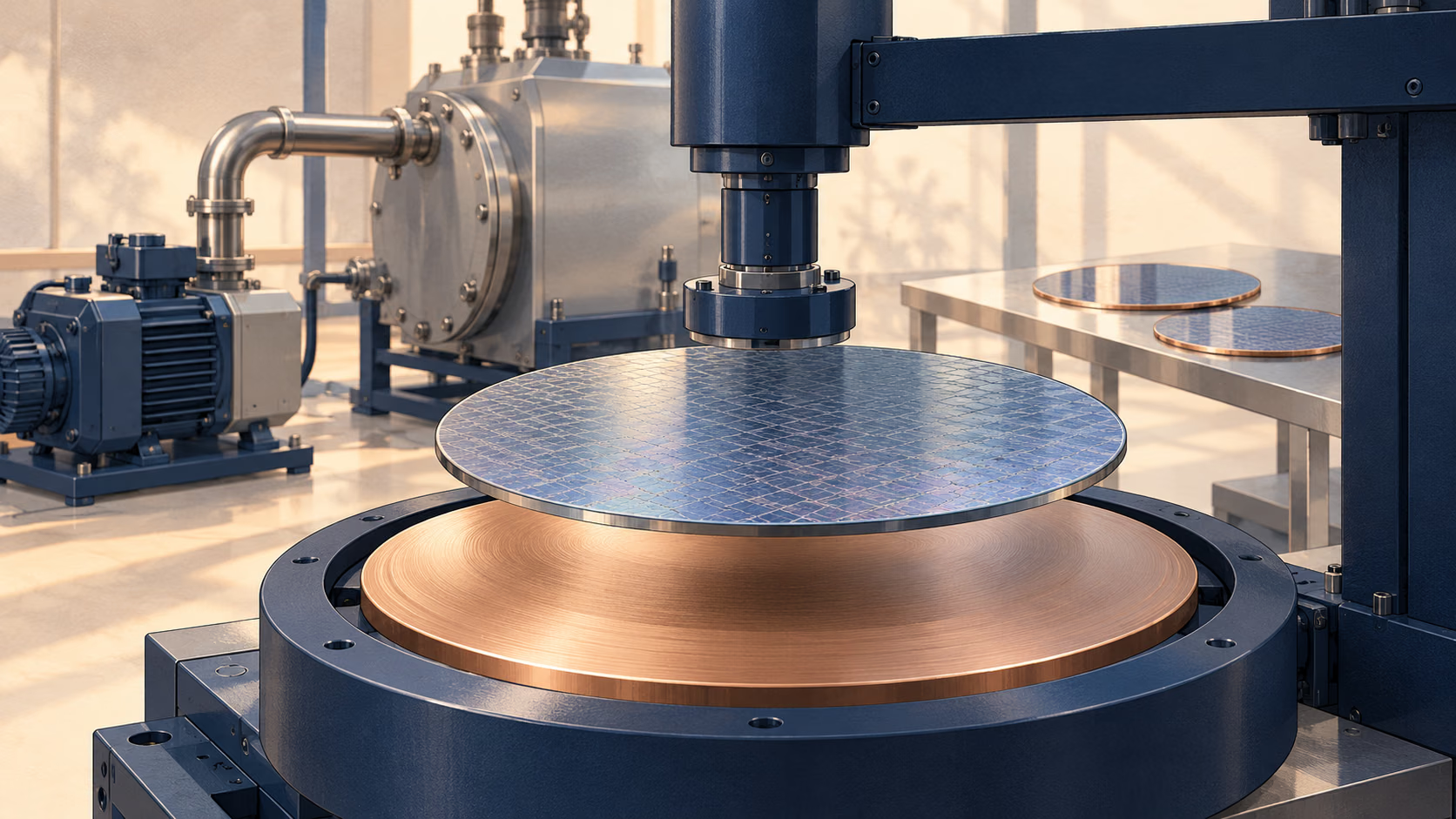
CMP stands for Chemical Mechanical Polishing and is used to planarize a wafer’s surface. Ebara’s integrated report places it not only in front-end circuit fabrication, but also in wafer bonding and advanced packaging.
DATA VIEW
CMP is the largest Precision Machinery revenue category
FY ended December 2025. Values in ¥bn; the three categories total ¥342.2bn.
A pump controls the space; a polishing system works on the material
The pump conditions the processing environment. A CMP system works on the wafer’s surface. They perform distinct jobs even when they serve the same semiconductor factory.
Gas in a chamber, a wafer surface and a wafer edge
Three schematic jobs in semiconductor manufacturing. This is not a complete, sequential production line.
Remove gas
A dry vacuum pump removes gas from the processing space. Ebara supplies chipmakers and equipment makers.
Flatten the surface
CMP systems planarize wafers. Ebara supplies these processing systems to chipmakers.
Prepare the edge
Bevel polishing works on the edge and rim, areas that also matter to subsequent bonding quality.
Shapes, dimensions and process order are schematic. Bonding is a separate operation from polishing. Downstream exhaust treatment is omitted.
Sources: Ebara Integrated Report 2026 (PDF pp.30, 33) and its dry vacuum pump explanation: PDF p.30 · PDF p.33 · Vacuum pump
Before wafers are bonded, their edges matter too
Work after delivery accounts for ¥97.0bn
CONCEPT MAP
Different jobs in a semiconductor factory
Customer production processesChipmakers / equipment makers
Processing environmentDry vacuum pumps remove gas
Wafer surfaces and edgesCMP and bevel systems process the material
After deliveryOverhauls, consumables, parts and repairs
A summary of roles, not a claim that every process uses the same equipment. Sources: Integrated Report PDF pp.30–33 and the dry vacuum pump explanation.
THE VIEW AFTER THE NUMBERS
What the numbers suggest
Ebara’s semiconductor business performs two distinct jobs: creating a vacuum in the processing space and polishing the wafer itself. In 2025, CMP represented 62% of Precision Machinery revenue.
As semiconductor structures become more layered and wafers are bonded, flat surfaces and clean edges become manufacturing challenges. Ebara supplies processing equipment and remains involved through parts and repairs. Its work reaches both the space around the wafer and the material being made into a chip.
JEOL’s electron-beam writers are used in making the gratings in DFB lasers for optical communications. Spot-beam orders and sales rose in the year ended March 2026, while fewer mask writers were sold and industrial-equipment sales declined. Following what each machine patterns, and where it sits in its customer’s production process, reveals different demand conditions within semiconductor-related equipment.